-
DFN/QFN lead frame packaingQFN package (square flat no pin package) and QFP package (square flat package): QFN and QFP packages based on copper lead frame, with a large exposed solder pad in the central area of the package for heat conduction, and conductive solder pads around the package periphery for electrical connection. Traditional chip packaging and integrated solutions with high reliability, high heat dissipation, and high density.


-
LGA carrier board packaging
LGA (Land Grid Array) is a packaging technology that utilizes a planar array of metal contacts (pads) on the bottom of the chip to establish electrical connections with corresponding pads on a printed circuit board (PCB) through soldering (e.g., reflow soldering) or sockets (e.g., CPU sockets). This design leverages the advantages of short contact points and electrical pathways to optimize high-frequency signal transmission performance. Additionally, direct contact between the bottom metal pads and the PCB enhances heat dissipation efficiency while supporting higher-density pin layouts, making it suitable for highly integrated, high-performance integrated circuit packaging applications.

-
BAG packaging
 Ball Grid Array (BGA) packaging: The interconnection between the chip and substrate is achieved through wire bonding (die bond/wire bond) of conventional face-up chips or advanced hybrid packaging (Hybrid BGA) combining face-up and flip-chip technologies. An array of solder balls is arranged on the backside of the package substrate to serve as I/O terminals for connecting with printed circuit boards (PCBs).
 -
Flip Chip PackagingThe core of Flip Chip lies in bump technology. During the manufacturing process of chips, metal bumps (such as solder balls, copper pillars+tin caps, etc.) are deposited on the I/O pads, and then the chip is flipped over to align the bumps with the corresponding pads on the substrate, achieving interconnection through reflow soldering. This design distributes the I/O terminals across the entire chip surface, significantly improving packaging density and signal transmission efficiency.

-
SiP system level packaging
 SiP (System in a Package): It has evolved from a conventional single chip with passive components to a multi chip multifunctional chip with passive components, covering hybrid packaging technologies including die bond/wire bond and flip chip, as well as other devices such as MEMS or optical sensor devices that are first assembled together to achieve a certain functional standard package, forming a system or subsystem.
 -
Chiplet Heterogeneous IntegrationHeterogeneous chip engine adopts Chiplet microsystem architecture, which encapsulates 7nm computing chips, 28nm I/O chips, and HBM3D stack through UCIe high-speed interface at once, achieving a 40% performance improvement and a 35% cost reduction, providing reusable and scalable heterogeneous power for AI servers.

01
Core Technology
Core Technology
-
 Simulation DesignWe have industry-leading joint design simulation technology and are skilled in optimizing the design of advanced packaging materials and simulation data. Provide customers with SI/PI electrical performance analysis, product structure stress and reliability analysis, heat dissipation performance analysis and thermal resistance extraction, plastic packaging& Bottom filling adhesive mold flow filling analysis, as well as three-level collaborative Co Design design and simulation services for the joint chip end packaging end system end.• Advanced Packaging Design Services• Electrical performance simulationanalysis technology• Structural stress simulation analysistechnology• SI/PI global electrical performanceverification;• Actuarial calculation of thermal resistancelevel heat dissipation performance;• Three level collaborative Co Design;• Multi physics field stress reliability prediction;• Simulation optimization of rubber materialmold flow filling;• Packaging mold flow filling analysis• Packaging heat dissipation simulationanalysis technology
 -
 Plastic encapsulation moldingPlace the epoxy resin encapsulation material particles in the injection channel of the mold, preheat them, and use the injection rod to transfer the melted epoxy resin into the mold cavity in a vacuum environment.• Advanced plastic packaging and moldingservices• Sealing thickness: 0.2-2.5mm Automaticsealing;• Real time monitoring and predictivemaintenance;• Good Core Grain (KGD) systemyield>95%;• &2-week process switching, supportingsmall batches and multiple varieties;• Warpage < 30 µ M @ 300mm wafer;• Unit wafer energy consumption reducedby 25%, carbon emissions traceable;• SPC and traceability system zero defectclosed-loop management;• 2.5-7.5mm manual sealing adhesive;• High density, large substrate, and thinthickness packaging;
 -
 Quality assuranceFull process quality assurance runs through the entire product lifecycle, relying on a sound quality management system to ensure high-quality products from development to delivery and after-sales. Develop a quality plan during the development phase and extensively validate it; Comprehensive testing and simulation during the introduction of new processes and products; Strict certification and testing of incoming materials; Fine process control; Multiple factory inspections; Trial production scientific improvement; Efficient after-sales service and continuous optimization, with the aim of customer satisfaction.• Systematic planning;• Strict incoming material control;• Rigorous factory inspection;• Efficient customer service;• Multi party review and supervision;• Scientific trial production improvement• Continuous improvement mechanism;• Data driven decision-making;• Fine process control• Comprehensive development verification
 -
 Delivery ServiceWe provide one-stop delivery services for chip packaging and testing, covering mainstream fields such as network communication, mobile terminals, high-performance computing, in vehicle electronics, big data storage, artificial intelligence and the Internet of Things, and industrial intelligent manufacturing; Relying on 7× The 24-hour response mechanism and full process traceability system ensure fast, accurate, and reliable delivery of multiple packaging forms, meeting customers' needs for mass production and market launch.• One stop testing delivery;• Full process traceability system;• Special Plan for NetworkCommunication;• High performance computingacceleration verification;• Big data storage reliability testing;• High yield guarantee for mobile terminals;• Vehicle grade AEC-Q100 certification• AIoT+Industrial Intelligent ManufacturingCustomization Service;• Compatible with multiple packaging forms;• 7× 24-hour rapid response;
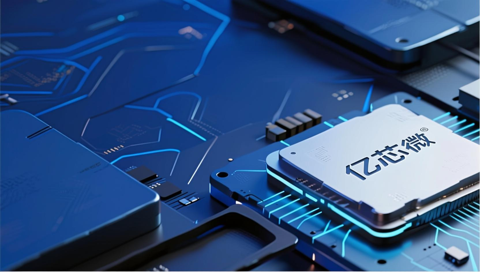
A high-tech company that leads the industry in advanced system level integrated packaging technology, always adheres to breakthroughs and innovations in core capabilities to meet customers' demands for high-end technology.
03
application field
Application Area
Focusing on providing higher reliability and more customized product solutions for application fields such as artificial intelligence, computing power products, automotive electronics supply chain, industrial control and new energy, and smart wearable devices
04
04

Mobile intelligent terminal
Providing highly reliable embedded storage packaging for mobile phones and wearable devices, ensuring low power consumption and fast startup.

smart home
Integrated sensor and storage packaging, enabling IoT devices to operate stably for long periods in complex environments.

smart car
Meets AEC-Q100 automotive-grade standards, provides wide-temperature-range storage and sensor packaging, supports real-time computing for autonomous driving

PC
Delivering high-capacity FCBGA memory and multi-chip SiP integration solutions for notebook and desktop platforms

data center
High-density heterogeneous integration technology meets the high-bandwidth and low-latency requirements of server-grade storage modules

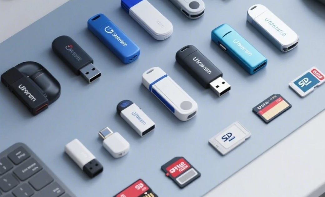
portable storage
Integrate packaging, modules, and PCBA into plug-and-play finished products to shorten the time-to-market for UFD and solid-state mobile hard drives
About Yixin Micro
About YCHIPWAY
05
Yixinwei Semiconductor Technology (Shenzhen) Co., Ltd. is a solution provider engaged in memory packaging & testing and module manufacturing, sensor packaging & testing and modules, etc. The company is located at 2-5C, Zhongcheng Biomedical Industrial Park, No. 21 Linhui Road, Jinsha Community, Kengzi Street, Pingshan District, Shenzhen, with convenient transportation and a beautiful environment. Since its establishment, the company has actively explored the market, continuously improved its R&D, production, and sales management systems, and is committed to creating an advanced semiconductor chip packaging & testing and module manufacturing enterprise, providing customers with a full-chain "one-stop" solution from chips to finished modules.
- The company has first-class office and production environments and management levels, with 1,500 square meters of Class 1,000 and 5,000 square meters of Class 10,000 clean rooms.
- The company has successively passed the ISO9001:2015 Quality Management System, ISO14001 Environmental Management System Certification, ISO45001 Occupational Health and Safety Management System, and IATF16949 International Automotive Industry Quality Management System Standard.
- The company encourages employees to innovate and develop their individuality in their work, providing excellent talents with broad career opportunities.
- Yixinwei Semiconductor Technology is a national high-tech enterprise and a national-level "Specialized, Refined, Distinctive, and Innovative" enterprise.
- Integrated R&D, packaging & testing, and module operations: integrating storage solution R&D, advanced packaging & testing, module assembly testing and services, and brand operations.
- Self-built advanced packaging & testing and module factories, specializing in memory chip packaging & testing, sensor chip packaging, multi-chip heterogeneous integration, QFN, FCBGA, and SiP, among other advanced packaging & testing fields.
- Two major product categories: embedded memory packaging & testing and sensor packaging & testing; one distinctive service: packaging + module assembly + PCBA solution finished product testing.
partner
Business Partners
06

News and Information
News Center
07
Scientific management, sincere service, innovation and improvement, meeting needs; Adhere to regulations and advocate for environmental protection; Ensure safety and maintain a harmonious home.


About Yixin Micro
Copyright© Yixin Micro Semiconductor Technology (Shenzhen) Co., Ltd; Guangdong ICP No. 2025459454-1
Address: 5C, Building 2, Zhongcheng Biomedical Industrial Park, No. 21 Linhui Road, Jinsha Community, Kengzi Street, Pingshan District, Shenzhen
Phone: 15307525582
Email: sales@ychipway.com
Product Center
Service and Support
Industry News
Contact Us
Scan to add enterprise WeChat